Source Code: GitHub
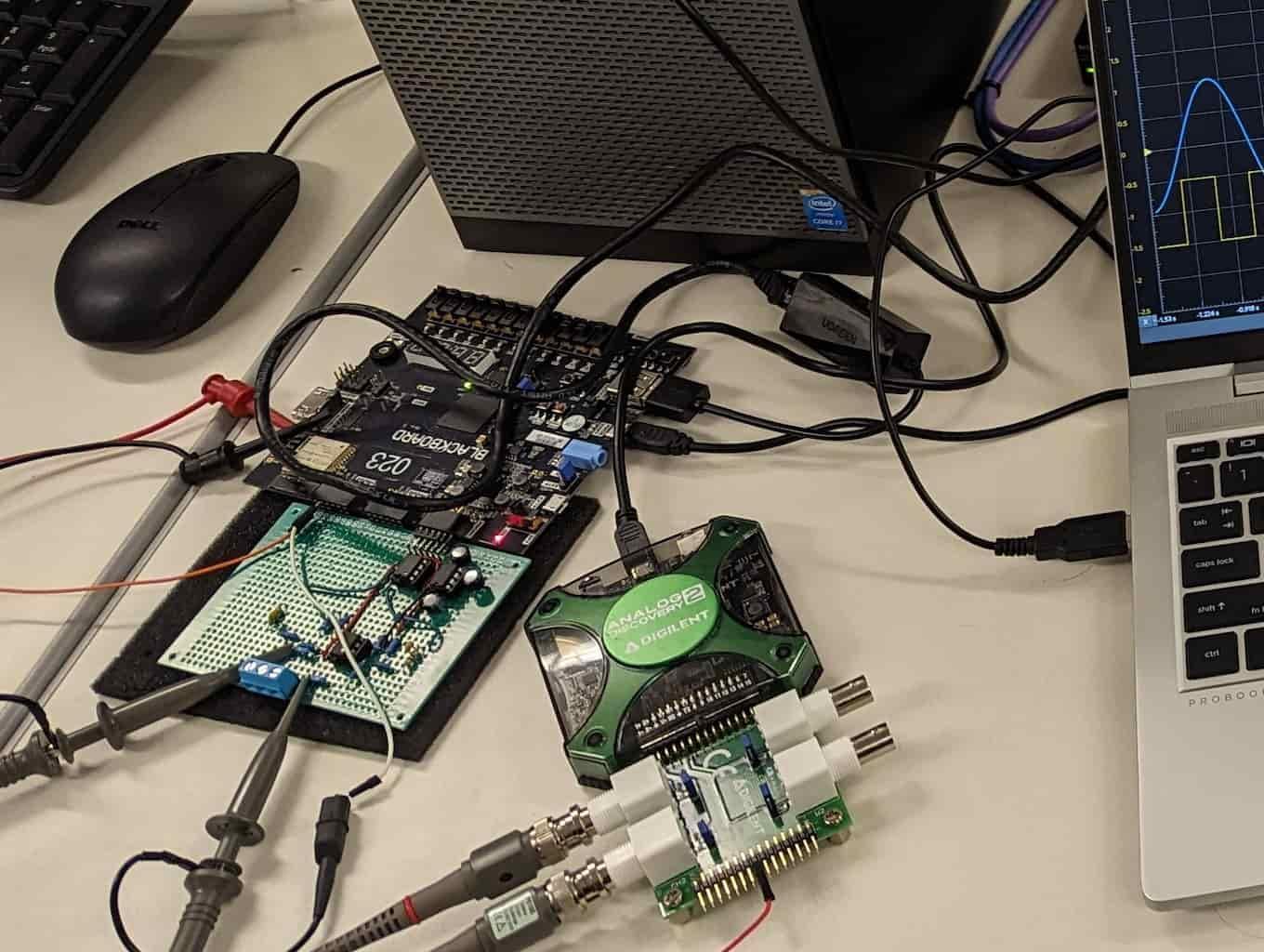
This project implemented a dual-channel waveform generator on a Xilinx Zynq based Real Digital Blackboard. There
were many components to this project, such as the external hardware used for the signal generator, the
SystemVerilog
code that was used to run that hardware and create data for the signal generator, and also the "system on chip"
part
of the project which used the Blackboard's ARM chip running Linux to control the hardware via a user-friendly
shell
terminal.
Unfortunately, there are no demos in this page as the Blackboard had to be returned. There are a few screenshots
that were taken as the project progressed showing some of its functions, however. All of the code is of course
also
available to view as to verify the project's functions.
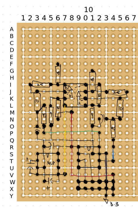
As stated previously, there is external hardware connected to the Real Digital Blackboard that was used in
creating
the signals. This includes a MCP4822 dual channel 12-bit digital to analog converter, an ICL7660 voltage
converter,
and a TLV2372 rail-to-rail op amp.
To the right is how I planned the external circuit, along with how it connected to the Blackboard. This was so
the
hardware could be soldered onto a small 5x7cm prototyping board and connected to the blackboard via a 2x7
right-angled pin header.
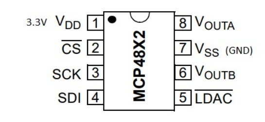
The MCP4822 a dual-channel 12-bit digital to analog converter that communicates via SPI and can output voltages from 0 to 2.047. The Blackboard was connected to it via its PMOD connectors, and a hardware implementation on an FPGA written in SystemVerilog was written to drive the DAC. More on this can be read in the software section of this page.
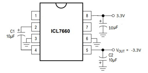
The ICL7660 is a voltage converter that takes a positive voltage and converts it to a negative voltage. This was used to create a negative voltage rail for the op amp, as the MCP4822 DAC only supplies positive voltage. This will allow signals to be able to peak from positive to negative voltage, otherwise the voltage floor would always be 0.
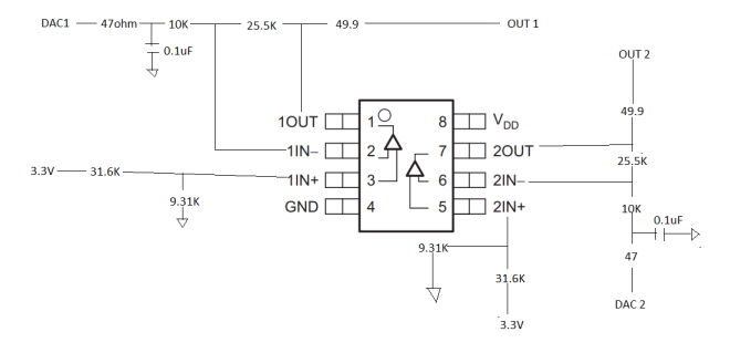
The TLV2372 is a rail-to-rail op amp that was used to buffer the signals from the DAC. This allows the signal generator to be able to output signals from negative to positive 2.5V. The resistor values were carefully chosen by our professor in order to make sure that the negative and positive voltages could be as close as they possibly could.
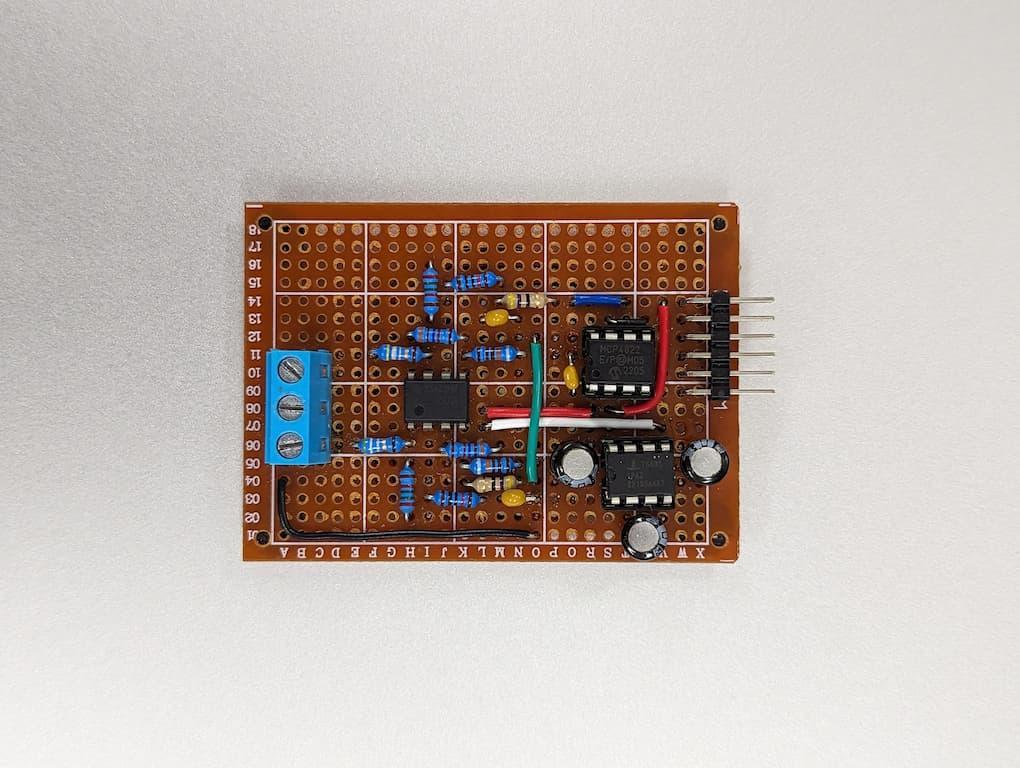
The SPI DAC driver was written in SystemVerilog and was used to drive the MCP4822 DAC. As stated previoulsly, the DAC is dual-channel and this driver does run both. It runs the DAC at an max rate of 100 KHz. Below, you can see the order in which each signal is meant to be pulled in order to run both outputs simultaneously.
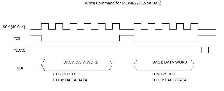
Fourty clocks were sent at a rate of 4 MHz to the DAC which is where the 100 KHz rate comes from. In terms
of a
state machine, there were six states in sending the data, which went as follows:
1) Idle for 2 clocks → 2) Send 16 bits for channel A → 3) Pull ~CS high for 4 clocks → 4) Send 16 bits for channel B → 5) Idle for 2 clocks → 6) Pull ~LDAC low and ~CS high, pull ~LDAC high at the end → 1) ...
This can be seen in the SystemVerilog code of the spi_engine.sv top-level module, starting at line 144
through
line
259. Since the code is very long, click here to see the code on GitHub.
The Wavegen IP is where the 12 bits that the SPI DAC needed were calculated. It has 8 32-bit registers that store various settings that affected the output of the signal generator, and were easily able to be written to using Linux programs that wrote to the registers of the module via the AXI-4 Lite bus.